counter for iweb
Website
Silicon Photonics

Published book, click here

Entries in PCI Express (6)

Monday
Aug072023

The long arm of PCI Express  

Optical is being added as a second physical medium to the PCI Express (PCIe) data transfer protocol.

PCI Express is an electrical standard, but now the Peripheral Component Interconnect Special Interest Group (PCI-SIG) has created a working group to standardise PCIe’s delivery optically.

PCI-SIG is already developing copper cabling specifications for the PCI Express 5.0 and 6.0 standards.
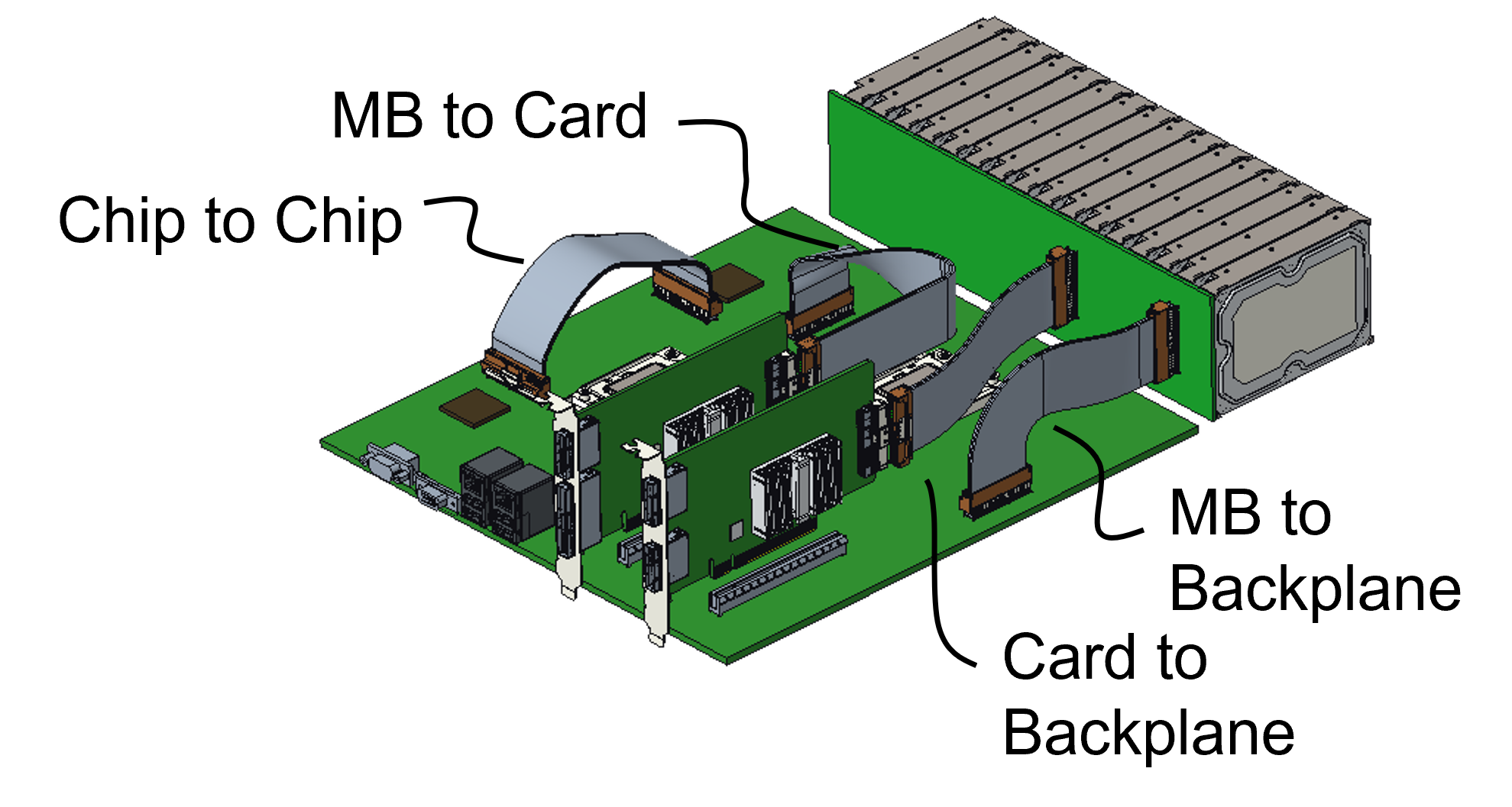
 

Source: PCI-SIG

Since each generation of PCIe doubles the data transfer rate, PCI-SIG member companies want copper cabling to help with the design of high-speed PCIe interconnects on a printed circuit board (PCB), between PCBs, and between racks (see diagram).

Click to read more ...

Friday
Dec242021

Data centre disaggregation with Gen-Z and CXL

Part 1: CXL and Gen-Z

  • The Gen-Z and Compute Express Link (CXL) protocols have been shown working in unison to implement a disaggregated processor and memory system at the recent Supercomputing 21 show.
  • The Gen-Z Consortium’s assets are being subsumed within the CXL Consortium. CXL will become the sole industry standard moving forward.
  • Microsoft and Meta are two data centre operators backing CXL.

Pity Hiren Patel, tasked with explaining the Gen-Z and CXL networking demonstration operating across several booths at the Supercomputing 21 (SC21) show held in St. Louis, Missouri in November.

Hiren Patel

Not only was Patel wearing a sanitary mask while describing the demo but he had to battle to be heard above cooling fans so loud, you could still be at St. Louis Lambert International Airport.

Gen-Z and CXL are key protocols supporting memory and server disaggregation in the data centre.

The SC21 demo showed Gen-Z and CXL linking compute nodes to remote ‘media boxes’ filled with memory in a distributed multi-node network (see diagram, bottom).

Click to read more ...

Friday
Oct052018

PCI Express back on track with latest specifications 

Richard Solomon and Scott Knowlton are waiting for me in the lobby of a well-known Tel-Aviv hotel overseeing the sunlit Mediterranean Sea.  

Richard SolomonSolomon, vice chair of the PCI Special Interest Group (PCI-SIG), and Knowlton, its marketing working group co-chair, are visiting Israel to deliver a training event addressing the PCI Express (PCIe) high-speed serial bus standard. 

With over 750 member companies, PCI-SIG conducts several training events around the world each year. The locations are chosen where there is a concentration of companies and engineers undertaking PCIe designs. “These are chip, board and systems architects,” says Solomon. 

PCI-SIG has hit its stride after a prolonged quiet period. The group completed the PCIe 4.0 standard in 2017, seven years after it launched PCIe 3.0. The PCIe 4.0 doubles the serial bus speed and with the advent of PCIe 5.0, it will double again.

Click to read more ...

Sunday
Jun282015

Altera’s 30 billion transistor FPGA 

  • The Stratix 10 features a routing architecture that doubles overall clock speed and core performance 
  • The programmable family supports the co-packaging of transceiver chips to enable custom FPGAs  
  • The Stratix 10 family supports up to 5.5 million logic elements
  • Enhanced security features stop designs from being copied or tampered with      

Altera has detailed its most powerful FPGA family to date. Two variants of the Stratix 10 family have been announced: 10 FPGAs and 10 system-on-chip (SoC) devices that include a quad-core 64-bit architecture Cortex-A53 ARM processor alongside the programmable logic. The ARM processor can be clocked at up to 1.5 GHz.

The Stratix 10 family is implemented using Intel’s 14nm FinFET process and supports up to 5.5 million logic elements. The largest device in Altera’s 20nm Arria family of FPGAs has 1.15 million logic elements, equating to 6.4 billion transistors. “Extrapolating, this gives a figure of some 30 billion transistors for the Stratix 10,” says Craig Davis, senior product marketing manager at Altera. 


Altera's HyperFlex routing architecture. Shown (pointed to by the blue arrow) are the HyperFlex registers that sit at the junction of the interconnect traces. Also shown are the adaptive logic module blocks. Source: Altera.

Click to read more ...

Wednesday
Dec102014

FPGAs embrace data centre co-processing role

Part 1: Xilinx's SDAccel development tool


The PCIe accelerator card has a power budget of 25W. Hyper data centres can host hundreds of thousands of servers whereas other industries with more specialist computation requirements use far fewers servers. As such, they can afford a higher power budget per card. Source: Xilinx

Xilinx has developed a software-design environment that simplifies the use of an FPGA as a co-processor alongside the server's x86 instruction set microprocessor.

Dubbed SDAccel, the development environment enables a software engineer to write applications using OpenCL, C or the C++ programming language running on servers in the data centre.   

Click to read more ...

Monday
Apr292013

NextIO simplifies top of rack switching with I/O virtualisation

NextIO has developed virtualised input/output (I/O) equipment that simplifies switch design in the data centre.


"Our box takes a single virtual NIC, virtualises that and shares that out with all the servers in a rack"

John Fruehe, NextIO 


The platform, known as vNET, replaces both Fibre Channel and Ethernet top-of-rack switches in the data centre and is suited for use with small one rack unit (1RU) servers. The platform uses PCI Express (PCIe) to implement I/O virtualisation.

Click to read more ...