
Monolithic silicon photonic chips move a step closer
Indium phosphide laser arrays have been grown on a 300 mm silicon wafer by Ghent University and imec, the Belgium nano-electronics R&D centre. Growing indium phosphide lasers directly onto the silicon wafer promises compact monolithic silicon photonics circuits.
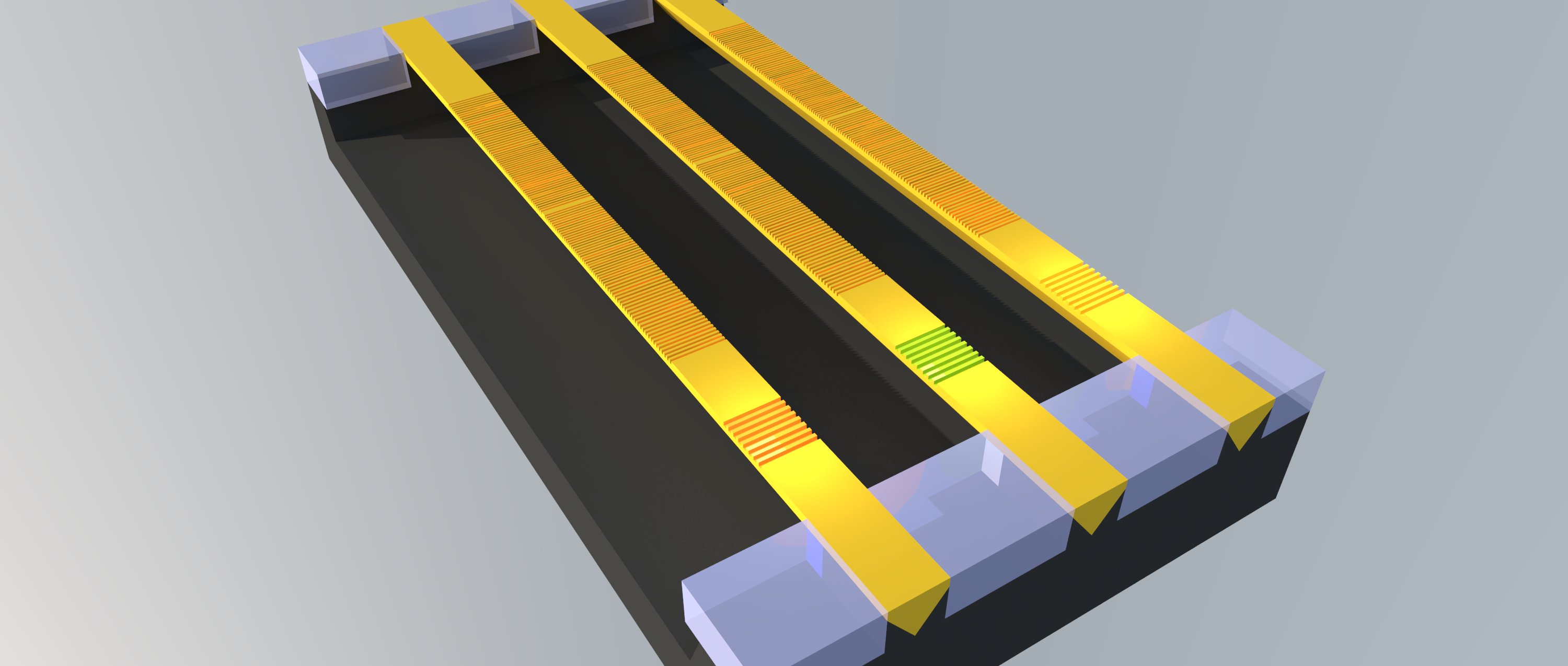 Shown are three v-shaped indium phosphide lasers and their gratings on a silicon-on-insulator substrate. Source: Ghent University, imec
Silicon photonics chips are hybrid designs because of silicon’s inability to generate light. Silicon photonics companies either couple a discrete laser to a chip or bond indium phosphide wafers or ‘chiplets' to the silicon wafer and process it to create working lasers that become part of the silicon photonics chip. Growing lasers directly on silicon creates a third approach for the densest applications.
 Post a Comment