counter for iweb
Website
Silicon Photonics

Published book, click here

Entries in CMOS (7)

Wednesday
May312017

Packaging silicon photonics using passive alignment  

  • An Israeli start-up is tackling a key packaging challenge for silicon photonics

Teramount has developed a way to simplify the packaging of silicon photonics chips. Instead of using active alignment whereby an external laser is required to carefully align a fibre to the optical die, the Israeli start-up has developed a technology that allows passive alignment.  


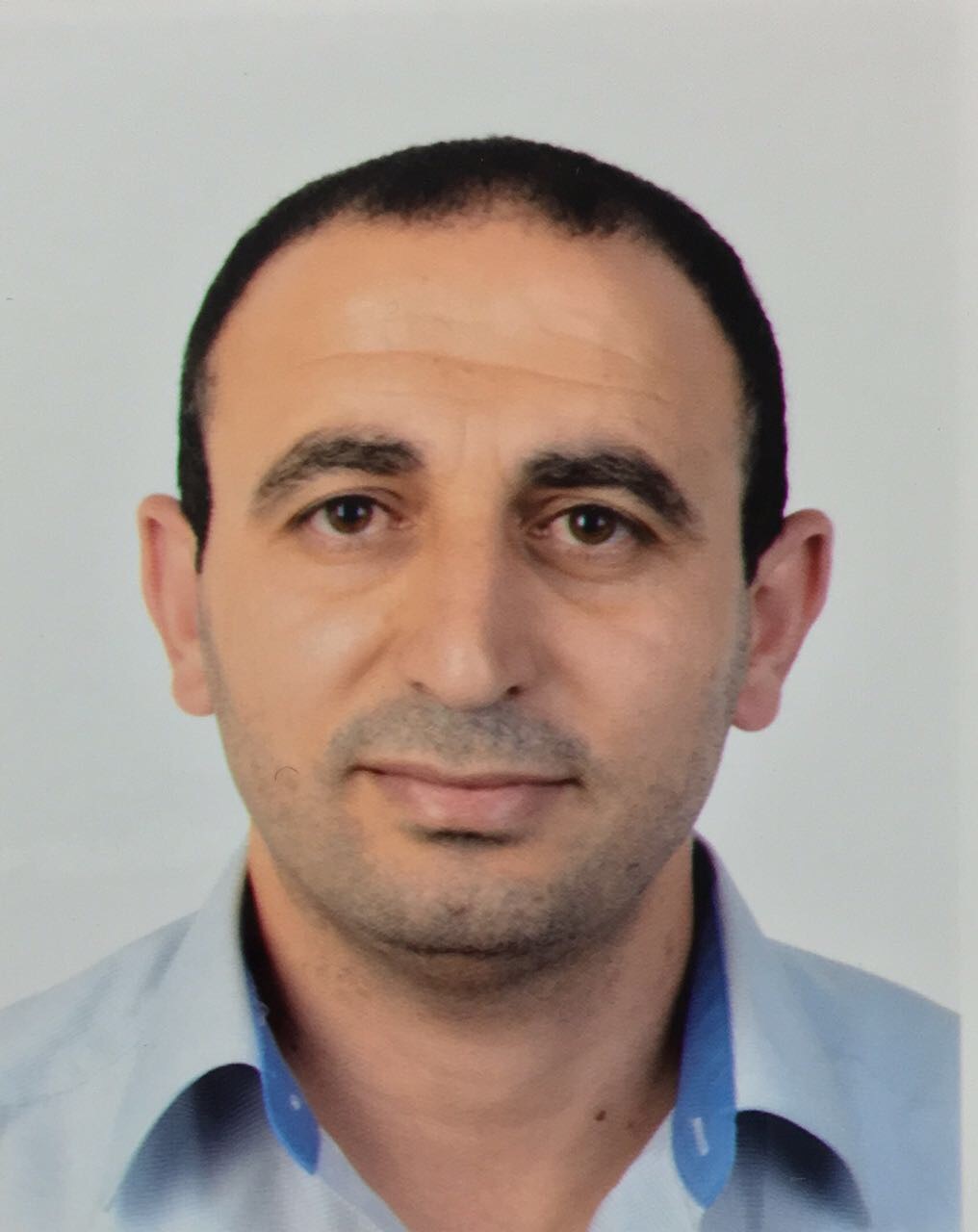
Hesham Taha“If we want silicon photonics to ramp up to volume, it has to meet CMOS standards both in terms of fabrication and packaging,” says Hesham Taha, Teramount's CEO.

Taha worked at a company developing atomic force microscopy systems before co-founding Teramount. "We got to know of the problem of injecting light into a waveguide and were surprised that the industry was still using active alignment," he says.

Click to read more ...

Sunday
Mar122017

IoT will drive chip design and new styles of computing

Looking back 20 years hence, how will this period be viewed? The question was posed by the CEO of imec, Luc Van de hove, during his opening talk at a day event imec organised in Tel-Aviv.

For Van den hove, this period will be seen as one of turbulent technological change. “The world is changing at an incredible rate,” he says. “The era of digital disruption is changing our industry and this disruption is not going to stop.”

Luc Van den hove

It was the Belgium nonoelectronics R&D centre’s second visit to Israel to promote its chip and systems expertise as it seeks to expand its links with Israel’s high-tech industry. And what most excites imec is the Internet of Things (IoT), the advent of connected smart devices that turn data into information and adapt the environment to our needs.

Click to read more ...

Tuesday
Mar082016

Silicon photonics adds off-chip comms to a RISC-V processor

A group of researchers have developed a microprocessor that uses silicon photonics-based optics to send and receive data.

"For the first time a system - a microprocessor - has been able to communicate with the external world using something other than electronics," says Vladimir Stojanovic, associate professor of electrical engineering and computer science at the University of California, Berkeley. 


Vladimir Stojanovic

The microprocessor is the result of work that started at MIT nearly a decade ago as part of a project sponsored by the US Defense Advanced Research Projects Agency (DARPA) to investigate the integration of photonics and electronics for off-chip and even intra-chip communications.  

Click to read more ...

Tuesday
Jun022015

Moore's law and silicon photonics

It is rare for a trade magazine article to receive so much coverage 50 years after publication. But then it is not often that an observation made in an article becomes a law, a law that explained how electronics would become a transformative industry. 

Chip pioneer Gordon E. Moore’s article appeared in the magazine Electronics in 1965. Dr. Moore was the director of the R&D labs at Fairchild Semiconductor, an early maker of transistors. Moore went on to co-found Intel, then a memory company, and became its second CEO after Robert Noyce. 

Moore’s article was written in the early days of integrated circuits. At the time, silicon wafers were one inch in diameter and integrating 50 components on a chip was deemed a state-of-the-art design

Click to read more ...

Tuesday
Jan132015

Graphene prototype modulator shown working at 10 Gigabit 

  • Imec's graphene electro-absorption modulator works at 10 Gigabit-per-second
  • The modulator is small and has be shown to be thermally stable
  • Much work is required to develop the modulator commercially


Cross-section of the graphene electro-absorption modulator. The imec work was first detailed in a paper at the IEDM conference held in December 2014 in San Francisco. Source: imec

Imec has demonstrated an optical modulator using graphene operating at up to 10 Gigabit. The Belgium nano-electronics centre is exploring graphene - carbon atoms linked in a 2D sheet - as part of its silicon photonics research programme investigating next-generation optical interconnect. Chinese vendor Huawei joined imec's programme late last year.

Click to read more ...

Wednesday
Dec112013

First silicon photonics devices from STMicro in 2014 

STMicroelectronics expects to have first silicon photonics products by mid-2014. The chip company announced the licensing of silicon photonics technology from Luxtera in March 2012. Since then STMicro has been developing its 300mm (12-inch) CMOS wafer manufacturing line for silicon photonics at its fab at Crolles, France.

Flavio Benetti, STMicroelectronics

"We think we are the only ones doing the processing in a 12-inch line," says Flavio Benetti, general manager of  mixed processes division at STMicroelectronics.

Click to read more ...

Thursday
Feb142013

Alcatel-Lucent demos dual-carrier Terabit transmission

"Without [photonic] integration you are doubling up your expensive opto-electronic components which doesn't scale"

Peter Winzer, Alcatel-Lucent's Bell Labs

Click to read more ...