

Is silicon photonics an industry game-changer?
Briefing: Silicon Photonics
Part 3: Merits, challenges and applications
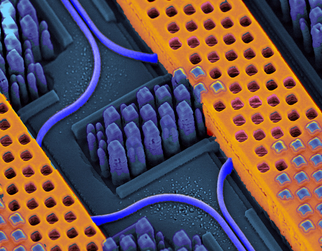 Shown in blue are the optical waveguides (and bend radius) while the copper wires carrying high-speed electrical signals are shown in orange. Source: IBM
System vendors have been on a silicon-photonics spending spree.
Cisco Systems started the ball rolling in 2012 when it acquired silicon photonics start-up, LightWire, for $272M. Mellanox Technologies more recently bought Kotura for $82M. Now Huawei has acquired Caliopa, a four-year-old Belgium-based start-up, for an undisclosed fee. The Chinese system vendor has said it is looking to further bolster its European R&D, and highlighted silicon photonics in particular.
Given that it was only just over a decade ago when systems companies were shedding their optical component units, the trend to acquire silicon photonics highlights the growing importance of the fledgling technology.
These system vendors view silicon photonics as a strategic technology. The equipment makers want to develop expertise and experience as they plan to incorporate the technology in upcoming, hopefully differentiated platforms.
"If I have a Terabit of capacity on the front panel, how am I going to manipulate that across the line card, a fabric or the backplane?" says Adam Carter, general manager and senior director of the transceiver modules group at Cisco Systems. "We saw silicon photonics as a technology that could potentially enable us to get there."
System vendors are already using embedded optics - mounted on boards close to the ICs instead of pluggable modules on the front panel - to create platforms with denser interfaces.
"Photonics doesn't need the latest and greatest lithography"
Arista Networks' 7500E switch has a line card with board-mounted optics rather than pluggable transceivers to increase 100 Gigabit port density. The company offers several line cards using pluggable modules but it has designed one card with board-mounted optics that offers flexible interfaces - 10 Gig, 40 Gig and 100 Gig - and a higher port density. When developing the design, the multi-source agreement (MSA) CFP2 pluggable module was not ready, says Arista.
Compass-EOS, a core IP router start-up, has developed chip-mounted optics based on 168 lasers and 168 detectors. The novel Terabit-plus optical interface removes the need for a switch fabric and the mid-plane to interconnect the router card within the platform. The interface also enables linking of platforms to scale the IP core router.
Both companies are using VCSELs, an established laser technology that silicon photonics competes with. Yet the two designs highlight how moving optics closer to chips enables system innovation, a development that plays to silicon photonics' strength.
 "I characterise silicon photonics as a technology that will compete in the right applications but won’t displace indium phosphide" Ed Murphy, JDSU
Silicon photonics promises cost savings by enabling vendors to piggyback on the huge investments made by the semiconductor industry. Vendors making their own products, such as optical transceivers, also promises to shake up the existing optical component supply chain.
Cisco Systems' first silicon photonics product is the proprietary 100 Gigabit optical CPAK transceiver that is undergoing qualification. By making its own optical module, Cisco avoids paying the optical module makers' margins. Cisco claims the CPAK's smaller size improves the faceplate density compared to the CFP2.
Pros and cons
Silicon photonics may be able to exploit the huge investment already made in the semiconductor industry, but it does differ from standard CMOS integrated circuits (ICs).
First, optics does not have the equivalent of Moore's Law. Whereas chip economics improve with greater integration, only a few optical functions can be cascaded due to the accumulated signal loss as light travels through the photonic circuit. This is true for optical integration in general, not just silicon photonics.
Another issue is that the size of an optical component - a laser or a modulator - is dictated by the laws of physics rather than lithography. "Photonics doesn't need the latest and greatest lithography," says Martin Zirngibl, domain leader for enabling physical technologies at Alcatel-Lucent's Bell Labs. "You can live with 100nm, 120nm [CMOS] components whereas for electronics you want to have 45nm."
This can lead to the interesting situation when integrating electronics with photonics. "You either don't use the latest technology for electronics or you waste a lot of real estate with very expensive lithography for photonics," says Zirngibl.
Another disadvantage of silicon is that the material does not lase. As a result, either a III-V material needs to be bonded to the silicon wafer or an external laser must be coupled to the silicon photonics circuit.
Silicon also has relatively small waveguides which make it tricky to couple light in and out of a chip.
The advantages of silicon photonics, however, are significant.
The technology benefits from advanced 8- and 12-inch wafers and mature manufacturing processes developed by the semiconductor industry. Using such CMOS processes promises high yields, manufacturing scale, and automation and testing associated with large scale IC manufacturing.
"This is probably the only advantage but it is very significant," says Valery Tolstikhin, founder and former CTO of indium phosphide specialist, OneChip Photonics, and now an independent consultant. "It takes silicon totally off the scale compared to any other photonics materials."
"We can build the single-die optical engine in the same CMOS line where processors are built, where billions [of dollars] of investment has been done"
IBM's high-density silicon photonics optical engine is made using a 90nm CMOS process. "We can build the single-die optical engine in the same CMOS line where processors are built, where billions [of dollars] of investment has been done," says Yurii Vlasov, manager of the silicon nanophotonics department at IBM Research. "We are riding on top of that investment."
Extra processing may be introduced for the photonics, says IBM, but the point is that there is no additional capital investment. "It is the same tooling, the same process conditions; we are changing the way this tooling is used," says Vlasov. "We are changing the process a little bit; the capital investment is in place."
 "We believe that even for shorter distance, silicon photonics does compete in terms of cost with VCSELs." Yurii Vlasov, IBM
Stephen Krasulick, CEO of silicon photonics start-up, Skorpios Technologies, makes a similar point. "The real magic with our approach is the ability to integrate it with standard, commercial fabs," he says.
Skorpios is a proponent of heterogeneous integration, or what the company refers to as 'silicon photonics 2.0'. Here silicon and III-V are wafer-bonded and the optical components are created by etching the two materials. This avoids the need to couple external lasers and to use active alignment.
"We do it in a manner such that the CMOS foundry is comfortable letting the wafer back into the CMOS line," says Krasulick, who adds that Skorpios has been working with CMOS partners from the start to ensure that its approach suits their manufacturing flow.
Applications
The first applications adopting silicon photonics span datacom and telecom: from short-reach interconnect in the data centre to 100 Gigabit-per-second (Gbps) long-distance coherent transmission.
Intel is developing silicon photonics technology to help spur sales of its microprocessors. The chip giant is a member of Facebook's Open Compute Project based on a disaggregated system design that separates storage, computing and networking. "When I upgrade the microprocessors on the motherboard, I don't have to throw away the NICs [network interface controllers] and disc drives," says Victor Krutul, director business development and marketing for silicon photonics at Intel. The disaggregation can be within a rack or span rows of equipment.
"Optical modules do not require state-of-the-art lithography or large scale photonic integration, but they do need to be coupled in and out of fibre and they need lasers - none of that silicon photonics has a good solution for"
Intel has developed the Rack Scale Architecture (RSA) which implements a disaggregated design. One RSA implementation for Facebook uses three 100Gbps silicon photonics modules per tray. Each module comprises four transmit and four receive fibres, each at 25Gbps. Each tray uses a Corning-developed MXC connector and its ClearCurve fibre that support data rates up to 1.6Tbps. “Different versions of RSA will have more or less modules depending on requirements," says Krutul.
Luxtera, whose silicon photonics technology has been used for active optical cables, and Mellanox's Kotura, are each developing 100Gbps silicon photonics-based QSFPs to increase data centre reach and equipment face plate density.
One data centre requirement is the need for longer reach links. VCSEL technology is an established solution but at 100Gbps its reach is limited to 100m only. Intel's 100Gbps module, operating at 1310nm and combined with Corning's MXC connector and ClearCurve multi-mode fibre, enables up to 300m links. But for greater distances - 500m to 2,000m - a second technology is required. Data centre managers would like one technology that spans the data centre yet is cost competitive with VCSELs.
"Silicon photonics lends itself to that," says Cisco's Carter. "If we drive the cost lower, can we start looking at replacing or future proofing your network by going to single mode fibre?"
 "There are places where silicon photonics will definitely win, such as chip-to-chip optical interconnects, and there are places where there is still a question mark, like fibre-optics interconnects." Valery Tolstikhin
IBM's 25Gbps-per-channel optical engine has been designed for use within data centre equipment. "We are claiming we have density based on optical scaling which is the highest in the industry, and we have done it using monolithic integration: optical devices are built side-by-side with CMOS," says Vlasov.
What is important, says Vlasov, is not so much the size of the silicon waveguide but how sharp its bend radius is. The bend radius dictates how sharply the light can be guided while remaining confined within the integrated circuit. The higher the light confinement, the smaller the bend radius and hence the overall circuit area.
Much progress has been made in improving light confinement over the past two decades, resulting in the bend ratio coming down from 1cm to a micron. IBM claims that with its technology, it can build systems comprising hundreds of devices occupying a millimeter. "That is a major difference in the density of optical integration," says Vlasov.
IBM does not use heterogeneous integration but couples lasers externally."It is not complicated, it is a technical problem we are solving; we believe that is the way to go," says Vlasov. "The reason why we have gone down this path is very simple: we believe in monolithic integration where electrical circuitry sits side by side with optical components."
Such monolithic integration of the optics with the electronics, such as modulator drivers and clock recovery circuitry, reduces significantly the cost of packaging and testing. "We believe that even for shorter distances, silicon photonics does compete in terms of cost with VCSELs if all elements of the cost are taken care of: bill of materials, packaging and testing," says Vlasov.
But not everyone believes silicon photonics will replace VCSELs.
For example, Tolstikhin questions the merits of silicon photonics for transceiver designs, such as for 100 Gig modules in the data centre. "There are places where silicon photonics will definitely win, such as chip-to-chip optical interconnects, and there are places where there is still a question mark, like fibre-optics interconnects," he says.
Tolstikhin argues that silicon photonics offers little advantage for such applications: "Optical modules do not require state-of-the-art lithography or large scale photonic integration, but they do need to be coupled in and out of fibre and they need lasers - none of that silicon photonics has a good solution for."
Cisco says it was first attracted to LightWire's technology because of its suitability for optical transceivers. Six years ago 1W, SFP+ modules were limited to 10km. "Customers wanted 40km, 80km, even WDM," says Carter. "They [LightWire] did a 40km SFP+ using their modulator that consumed only 0.5W - a huge differentiator." Two years ago 100 Gig CFP modules were at 24W while LightWire demonstrated a module under 8W, says Carter.
Tolstikhin believes silicon photonics' great promise is for applications still to emerge. One example is chip-to-chip communication that has modest optical light requirements and does not have to be coupled in and out of fibre.
"Here you have very high requirements for density packaging and the tiny [silicon] waveguides are handy whereas indium phosphide is too big and too expensive here," says Tolstikhin. Longer term still, silicon photonics will be used for on-chip communication but that will likely be based on deep sub-wavelength scale optics such as surface plasmonics rather than classical dielectric waveguides.
Tolstikhin also argues that the economics of using indium phosphide compared to silicon photonics need not be all that gloomy.
Indium phosphide is associated with custom small-scale fabs and small volume markets. But indium phosphide can benefit from the economics of larger industries just as silicon photonics promises to do with the semiconductor industry.
Indium phosphide is used in higher volume for wireless ICs such as power amplifiers. "Quite significantly orders of magnitude higher," says Tolstikhin. The issue is that, conventionally, photonic circuits are fabricated by using multiple epitaxial growth steps, whereas the wireless ICs are made in a single-growth process, hence epitaxy and wafer processing are decoupled.
"If you can give up on regrowth and still preserve the desired photonic functionality, then you can go to commercial RF IC fabs," he says. "This is a huge change in the economic model." It is an approach that enables a fabless model for indium phosphide photonics, with the potential advantages not unlike those claimed by silicon photonics with respect to commercial CMOS fabs.
"That suggests indium phosphide - which has all kinds of physical advantages for those applications that require transmitters, receivers and fibre, plus readily available high-speed analogue electronics for trans-impedance amplifiers and laser or modulator drivers - may be quite a competitive contender," says Tolstikhin.
"Silicon photonics has a certain capability but the hype around it has magnified that capability beyond reality"
Customers don't care which technology is used inside a transceiver. "They care only about cost, power and package density," says Tolstikhin. "Indium phosphide can be competitive and on many occasions beat silicon photonics."
JDSU also believes that long-term, a perfect fit for silicon photonics may be relative short reach interconnects – chip-to-chip and board-to-board reaches. “You need to have very high speed and dense interconnects, I can see that as being a very strong value proposition long term," says Ed Murphy, senior director, communications and commercial optical products at JDSU.
Finisar and JDSU are open to the potential benefits of silicon photonics but remain strong proponents of traditional optical materials such as indium phosphide and gallium arsenide.
"We have designed silicon photonic chips here at Finisar and have evaluations that are ongoing. There are many companies that now offer silicon photonics foundry services. You can lay out a chip and they will build it for you," says Jerry Rawls, executive director of Finisar. "The problem is we haven't found a place where it can be as efficient or offer the performance as using traditional lasers and free-space optics."
"Silicon photonics has a certain capability but the hype around it has magnified that capability beyond reality,” says JDSU's Murphy. "Practitioners of silicon photonics would tell you that as well."
According to Murphy, each application, when looked at in detail, has its advantages and disadvantages when using either silicon photonics or indium phosphide. “Even in those applications where one or the other is better, the level of improvement is measured in a few tens of percent, not factors of ten,” he says. "I characterise silicon photonics as a technology that will compete in the right applications but won’t displace indium phosphide."
Silicon photonics for telecom
At the other extreme of the optical performance spectrum, silicon photonics is being developed for long-distance optical transmission. The technology promises to help shrink coherent designs to fit within the CFP2 module, albeit at the expense of reach. A CFP2 coherent module has extremely challenging cost, size and power requirements.
Teraxion is developing a coherent receiver for CFP2. "We believe silicon photonics is the material of choice to fulfill CFP2 requirements while allowing even smaller size reduction for future modules such as the CFP4," said Martin Guy, Teraxion's vice president of product management and technology.
u2t Photonics and Finisar recently licensed indium phosphide modulator technology to help shrink coherent designs into smaller form factor pluggables. So what benefit does silicon photonics offer here?
"In terms of size there will not be much difference between indium phosphide and silicon photonics technology," says Guy. "However, being on each side on the fence, we know that process repeatability and therefore yield is better with silicon photonics." Silicon photonics thus promises a lower chip cost.
"We have projects spanning everything from access all the way to long haul, and covering some datacom as well," says Rob Stone, vice president of marketing and program management at Skorpios. The start-up has developed a CMOS-based tunable laser with a narrow line width that is suitable for coherent applications.
"If you develop a library of macrocells, you can apply them to do different applications in a straightforward manner, provided all the individual macrocells are validated," says Stone. This is different to the traditional design approach.
Adding a local oscillator to a coherent receiver requires a redesign and a new gold box. "What we've got, we can plug things together, lay it out differently and put it on a mask," says Stone. "This enables us to do a lot of tailoring of designs really quite quickly - and a quick time-to-market is important."
Perhaps the real change silicon photonics brings is a disruption of the supply chain, says Zirngibl.
An optical component maker typically sells its device to a packaging company that puts it in a transmitter or receiver optical sub-assembly (TOSA/ ROSA). In turn, the sub-assemblies are sold to a module company which then sells the optical transceiver to an equipment vendor. Each player in the supply chain adds its own profit.
Silicon photonics promises to break the model. A system company can design its own chip using design tools and libraries and go to a silicon foundry. It could then go to a packaging company to make the module or package the device directly on a card, bypassing the module maker altogether.
Yet the ASIC model can also benefit module makers.
IBM has developed its 25Gbps-per-channel silicon photonics technology for its platforms, for chip-to-chip and backplanes, less for data centre interconnect. But it is open to selling the engine to interested optical module players. "If this technology can be extended to 2km for big data centres, others can come in, the usual providers of transceivers," says Vlasov.
"There are companies with the potential to offer a [silicon photonics] design service or foundry service to others that would like to access this technology," says Cisco's Carter. "Five years ago there wasn't such an ecosystem but it is developing very fast."
The article is an extended version of one that appeared in the exhibition magazine published at ECOC 2013.
Part 1: Optical interconnect, click here
Part 2: Bell Labs on silicon photonics, click here
 Post a Comment
Reader Comments