
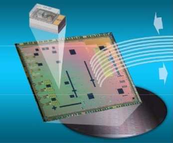
Luxtera's 100 Gigabit silicon photonics chip
Luxtera has detailed a 4x28 Gigabit optical transceiver chip. The silicon photonics company is aiming the device at embedded applications such as system backplanes and high-performance computing (HPC). The chip is also being used by Molex for 100 Gigabit active optical cables. Molex bought Luxtera's active optical cable business in January 2011.

“Do I want to invest in a copper backplane for a single generation or do I switch over now to optics and have a future-proof three-generation chassis?”
Marek Tlalka, Luxtera
What has been done
To make the optical transceiver, a distributed-feedback (DFB) laser operating at 1490nm is coupled to the silicon photonics CMOS-based chip. One laser only is required to serve the four individually modulated 28Gbps transmit channels, giving the chip a 112Gbps maximum data rate. There are also four receive channels, each using a germanium-based photo-detector that is grown on-chip.
The DFB is the same laser that Luxtera uses for its 4x10Gbps and 4x14Gbps designs. What has been changed is the Mach-Zehnder waveguide-based modulators that must now operate at 28Gbps, and the electronics amplifiers at the receivers. “The chip [at 5mmx6mm] is pretty much the same size as our 4x10 and 4x14 Gig designs,” says Marek Tlalka, director of marketing at Luxtera.
 Source: Luxtera
Luxtera is announcing the 100 Gigabit chip which it is sampling to customers. Molex, for example, will package the chip and the laser to make its active optical cable products. Luxtera will package the transceiver chip and laser in a housing as an OptoPHY, a packaged product it already provides at lower speeds. The company will sell the 100Gbps OptoPHY for embedded applications such as system backplanes and HPC.
Applications
The 100GbE transceiver chip is targeted at next-generation backplane applications as well as active optical cables. And it is enterprise vendors that make switches, routers and blade servers that are considering adopting optical backplanes for their next-generation platforms, says Luxtera.
According to Tlalka, system vendors are moving their backplanes from 15Gbps to 28Gbps: “It is pretty obvious that building an electrical backplane at this data rate will be extremely challenging.”
When vendors design a new chassis, they want it to support three generations of line cards. Even if a system vendor develops a 28Gbps copper-based backplane, it will need to go optical when the backplane data rate increases to 40-50Gbps in 2-3 years’ time and 100Gbps when that speed transition occurs. “Do I want to invest in a copper backplane for a single generation or do I switch over now to optics and have a future-proof three-generation chassis?” says Tlalka.
Exascale computers, 1000x more powerful than existing supercomputers planned for the second half of the decade, is another application area. Here there is a need for 25-28Gbps links between chips, says Tlalka.
System platforms and HPC are ideal candidates for the packaged transceiver chip but longer term Luxtera is eyeing the move of optics inside chips such as ASICs. Such system-on-chip optical integration could include Ethernet switch ICs (See example switch ICs from Broadcom and Intel (Fulcrum)) and network interface cards. Another example highlighted by Tlalka is CPU-memory interfaces.
However such applications are at least five years away and there are significant hurdles to be overcome. These include resolving the business model of such designs as well as the technical challenges of coupling the ASIC to the optics and the associated mechanical design.
Standards
Luxtera's 100Gbps transceiver chip supports a variety of standards.
Operating at 25Gbps per channel, the chip supports 100GbE and Enhanced Data Rate (EDR) Infiniband. The ability to go to 28Gbps per channel means that the transceiver can also support the OTN (optical transport network) standard as well as proprietary backplane protocols that add overhead to the basic 25Gbps data rate.
In addition the chip supports the OIF's short reach and very short reach interfaces that define the interface between an ASIC and the optical module.
The chip is also suited for some of the IEEE Next Generation 100Gbps Optical Ethernet Study Group standards now in development. These interfaces will cover a reach of 30m to 2km.
400GbE and HDR Infiniband
Luxtera says that it is working on different channel ’flavours' of 100G. It is also following developments such as Infiniband Hexadecimal Data Rate (HDR) and 400GbE.
HDR will use 40Gbps channels while there is still an industry debate as to whether 400GbE will be implemented using ten channels, each at 40Gbps, or as a 16x25Gbps design.
 Post a Comment
Reader Comments