counter for iweb
Website
Silicon Photonics

Published book, click here

Entries in imec (13)

Tuesday
Jul262016

The ecosystem for silicon photonics starts to take shape

Silicon photonics luminaries series


Interview 6: imec - Philippe Absil and Joris Van Campenhout


Imec has a unique vantage point when it comes to the status and direction of silicon photonics.  

The Belgium nano-electronics research centre gets to see prototype designs nearing commercialisation due to its silicon photonics integration platform and foundry service. “We allow companies to build prototypes using a robust silicon photonics technology,” says Philippe Absil, department director for 3D and optical technologies at imec.


Philippe Absil

Imec also works intimately with several partners on longer-term research, one being Huawei. This optical I/O R&D activity is part of imec’s CORE CMOS scaling R&D programme which as well as Huawei includes GlobalFoundries, Intel, Micron, Qualcomm, Samsung, SK Hynix, Sony and TSMC. The research is sufficiently far ahead to be deemed pre-competitive such that all the firms collaborate. 

For silicon photonics, the optical I/O research includes optical integration schemes, new device concepts and new materials. “The aim is to bring silicon photonics technology to the next level in order to resolve today’s challenges,” says Absil.  

Click to read more ...

Monday
May232016

Mario Paniccia: We are just at the beginning

Silicon photonics luminaries series
Interview 2: Mario Paniccia
 
Talking about his time heading Intel’s silicon photonics development programme, Mario Paniccia, spotlights a particularly creative period between 2002 and 2008.  
 
During that time, his Intel team had six silicon photonics papers published in the science journals, Nature and Nature Photonics, and held several world records - for the fastest modulator, first at 1 gigabit, then 10 gigabit and finally 40 gigabit, the first pulsed and continuous-wave Raman silicon laser, the first hybrid silicon laser working with The University of California, Santa Barbara, and the fastest silicon germanium photo-detector operating at 40 gigabit.
 
“These [achievements] were all in one place, labs within 100 yards of each other; you had to pinch yourself sometimes,” he says.

Click to read more ...

Thursday
Mar032016

Imec gears up for the Internet of Things economy  

Luc Van den hove is talking in the darkened ballroom in a hotel next to the brilliantly sunlit marina in Herzliya.

It is the imec's CEO's first trip to Israel and around us the room is being prepared for an afternoon of presentations the Belgium nanoelectronics research centre will give on its work in such areas as the Internet of Things and 5G wireless to an audience of Israeli start-ups and entrepreneurs.


Luc Van den hoveImec announced in February its plan to merge with iMinds, a Belgium research centre specialising in systems software and security, a move that will add 1,000 staff to imec's 2,500 researchers.

At first glance, the world-renown semiconductor process technology R&D centre joining forces with a systems house is a surprising move. But for Van den hove, it is a natural development as the company continues to grow from its technology origins to include systems-based research.

Click to read more ...

Wednesday
Nov112015

Monolithic silicon photonic chips move a step closer  

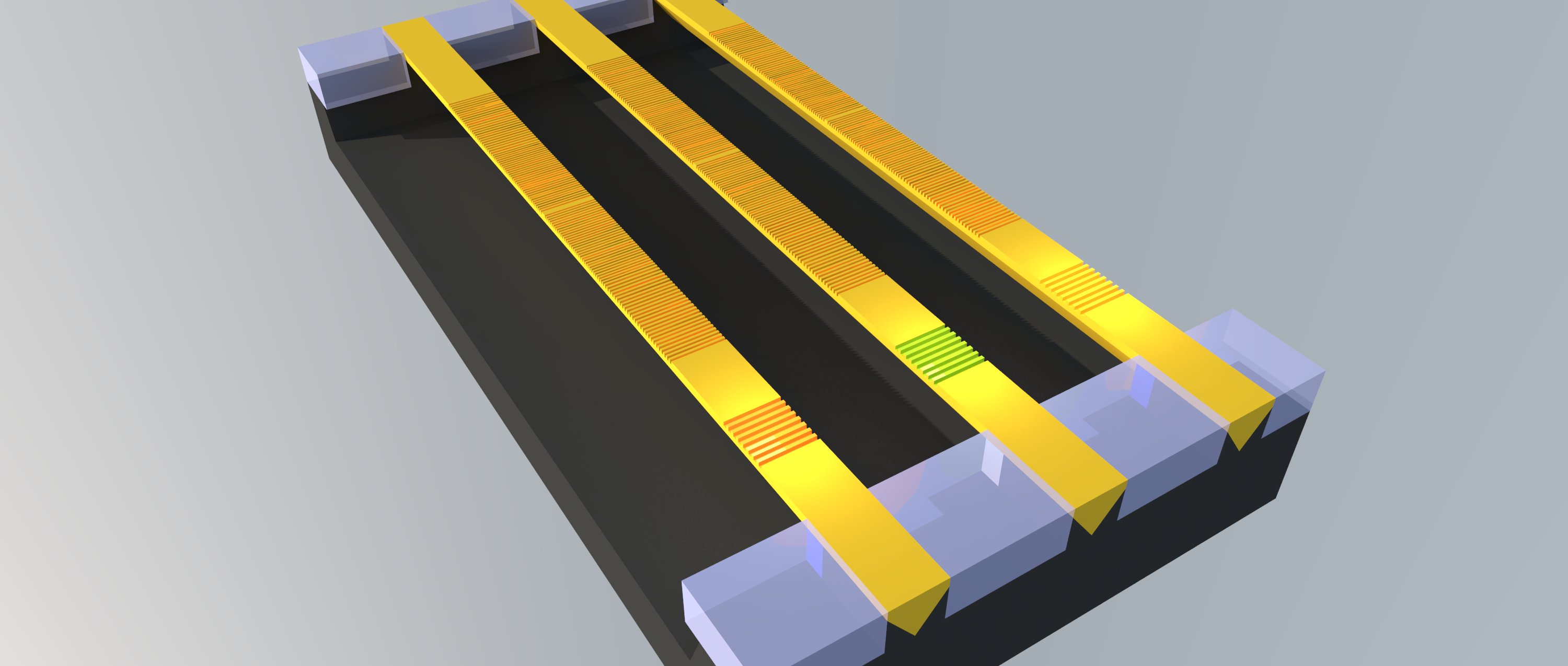
Indium phosphide laser arrays have been grown on a 300 mm silicon wafer by Ghent University and imec, the Belgium nano-electronics R&D centre. Growing indium phosphide lasers directly onto the silicon wafer promises compact monolithic silicon photonics circuits.   


Shown are three v-shaped indium phosphide lasers and their gratings on a silicon-on-insulator substrate. Source: Ghent University, imec

Silicon photonics chips are hybrid designs because of silicon’s inability to generate light. Silicon photonics companies either couple a discrete laser to a chip or bond indium phosphide wafers or ‘chiplets' to the silicon wafer and process it to create working lasers that become part of the silicon photonics chip. Growing lasers directly on silicon creates a third approach for the densest applications.

Click to read more ...

Tuesday
Jan132015

Graphene prototype modulator shown working at 10 Gigabit 

  • Imec's graphene electro-absorption modulator works at 10 Gigabit-per-second
  • The modulator is small and has be shown to be thermally stable
  • Much work is required to develop the modulator commercially


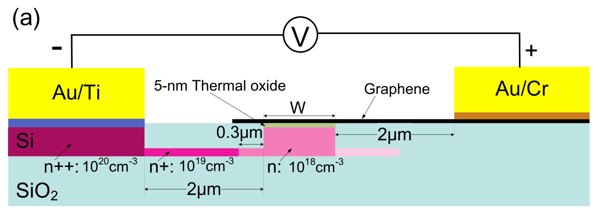
Cross-section of the graphene electro-absorption modulator. The imec work was first detailed in a paper at the IEDM conference held in December 2014 in San Francisco. Source: imec

Imec has demonstrated an optical modulator using graphene operating at up to 10 Gigabit. The Belgium nano-electronics centre is exploring graphene - carbon atoms linked in a 2D sheet - as part of its silicon photonics research programme investigating next-generation optical interconnect. Chinese vendor Huawei joined imec's programme late last year.

Click to read more ...

Friday
Dec192014

Huawei joins imec to research silicon photonics

Huawei has joined imec, the Belgium nano-electronics research centre, to develop optical interconnect using silicon photonics technology. The strategic agreement follows Huawei's 2013 acquisition of former imec silicon photonics spin-off, Caliopa.


Source: Gazettabyte

Click to read more ...

Page 1 2